


We can provide high temperature superconducting thin film substrate , magnetic thin films and ferroelectric thin film substrate , semiconductor crystal , optical crystal , laser crystal materials ,at the same time provide orientation and foreign universities and research institutes to provide high quality ( ultra smooth ,ultra smooth , ultra clean)
Maideli Wafer : Silicon Wafer Cutting

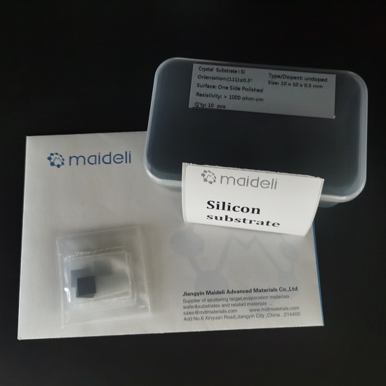
| Production Method | CZ |
| Length x Width | 10mm x 10mm ; 5mm x 5mm ; 15mm x15mm ;etc... |
| Thickness | 100um ,200um ,300 um ,400 um ,500 um ,600 um , 700um ,800 um ,900um ,1000um |
| Type | N type / P type |
| Orientation | <111> , <100>,<110> |
| Resistivity | 0.002~25000 Ω.cm |
| Flatness TIR | <3um |
Warping degree TTV | <10um |
flexibility BOW | <10um |
| Roughness | <0.5nm |
| Granularity | <10 ( for size >0.3um) |
| Application | Used for synchrotron radiation sample carrier, PVD/CVD coating as substrate, magnetron sputtering growth sample, XRD, SEM,Atomic force, infrared spectroscopy, fluorescence spectroscopy and other analysis test substrates, molecular beam epitaxial growth substrates, X-ray analysis of crystalline semiconductors |
Please send us your request with below details to " sales@mdlmaterials.com"
1. Size with tolerance (Length/Width/ Thickness )
2. Type ( N or P type )
3. Orientation
4. Electrical resistivity
5. Polishing Side (SSP or DSP )
6. Quantity


