


We can provide high temperature superconducting thin film substrate , magnetic thin films and ferroelectric thin film substrate , semiconductor crystal , optical crystal , laser crystal materials ,at the same time provide orientation and foreign universities and research institutes to provide high quality ( ultra smooth ,ultra smooth , ultra clean)
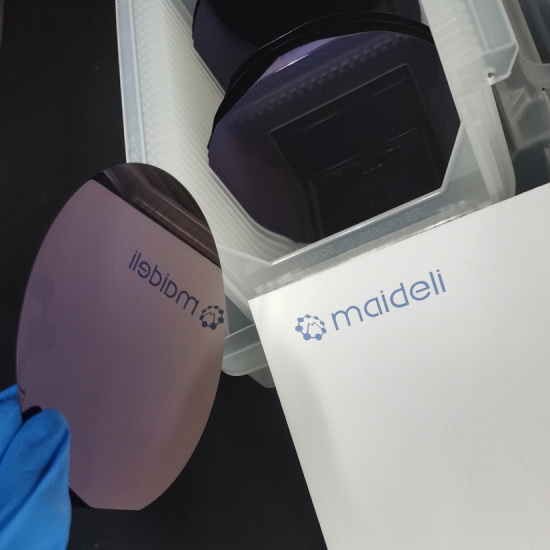
Product Name | Prime Grade 4 Inch SiO2 Wafer Silicon + SiO2 Layer Oxidized Wafer |
Material | Silicon |
Diameter | 4 Inch |
Thickness | 100-1000um |
Resistivity | <0.0015Ω●cm , 0.001~0.01Ω●cm , 1~5Ω●cm , 1~10Ω●cm , 10~20Ω●cm ,>1000Ω●cm,>10000Ω●cm |
Orientation | 100/110/111 |
Grade | Prime |
Growth | CZ |
Surface Finish | SSP |
Flats | SEMI-Std |
Type | P or N |
Layer thickness | 100nm/300nm (As requested ) |
Warp | <30um |
Particles | <15@0.3 |
Regular Type with Stock
| Single Side Polished + Both Sides Oxidation | 50nm | 100nm | 200nm | 285nm |
| 300nm | 500nm | 1000nm | 2000nm | |
| Single Side Polished + One Side Oxidation | 100nm | 200nm | 285nm | 300nm |
| 500nm | 1000nm | 2000nm | ||
| Both Sides Polished + Both Sides Oxidation | 100nm | 200nm | 285nm | 300nm |
| 500nm | 1000nm | 2000nm |

Please send us your request with below details to " sales@mdlmaterials.com"
1. Size with tolerance (Diameter / Thickness /oxidation layer thickness )
2. Type ( N or P type )
3. Orientation
4. Electrical resistivity
5. Polishing Side (SSP or DSP )
6. Quantity


