


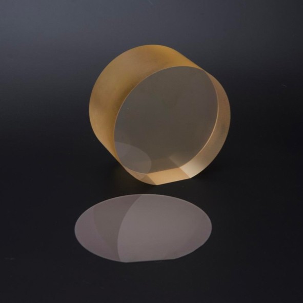


Maideli Lithium Niobate
| Material | Lithium Niobate |
| Orientation | X/Z/Y41°/Y64°/Y128°/YZ/YX or Customized |
| Diameter | 3" 4" 6" 8" LN wafer |
| Thickness | 0.18/0.25/0.35/0.50/1.00 + mm |
| Grade | Saw/Optical grade |
| Surface finish | single or double sides polish (DLP/SLP/ SSP/DSP all available ) |
| TTV | < 1~5μm |
| BOW | ± (25μm ~40um ) |
| Warp | <= 35μm |
| LTV (5mmx5mm) | <1.5 um |
| PLTV(<0.5um) | ≥98% (5mm*5mm) with 2mm edge excluded |
| Curie Temp | 1142°C±3°C |
| Edge | Compl't with SEMI M1.2@with GC800# .regular at C typed |
| Orientation flats | available, per request |
| Doped with | Zn, MgO single or double doped available |
| Polished side Ra | Roughness Ra<=5A |
| Back Side Criteria | Roughness Ra:0.5-1.0μm GC#1000 |
| Edge Rounding | Compliant with SEMI M1.2 Standard/refer to IEC62276 |
| Cracks, saw marks, stains | None |
| Single Domain | Completed Polarization/Reducted |
| Application | RF Saw filters and Optical parts usage |
Please send us your request with below details to “sales@mdlmaterials.com”
Size (Length / Width /Thickness)
Orientation
Polishing Side (SSP or DSP )


