


 wafers")
 wafers")
 wafers")

We can provide high temperature superconducting thin film substrate , magnetic thin films and ferroelectric thin film substrate , semiconductor crystal , optical crystal , laser crystal materials ,at the same time provide orientation and foreign universities and research institutes to provide high quality ( ultra smooth ,ultra smooth , ultra clean
Thermal oxidation is the result of exposing a silicon wafer to a combination of oxidizing agents and heat to make a layer of silicon dioxide (SiO2).Our company can customize silicon dioxide oxide flakes with different parameters for customers, with excellent quality; the oxide layer thickness, compactness, uniformity and resistivity crystal orientation are all implemented in accordance with national standards.
A silicon dioxide layer is formed on the surface of the thermal oxide. In the presence of an oxidant at an elevated temperature, the process is called thermal oxidation. The thermal oxide layer is usually grown in a horizontal tube furnace. The temperature range is controlled at 900 to 1200 degrees Celsius, using wet or dry growth methods. Thermal oxide is a growing oxide layer. Compared with the oxide layer deposited by CVD method, it has higher uniformity and dielectric strength. This is a dielectric layer of an insulator. In most silicon-based devices, the thermal oxide layer plays a very important role to comfort the surface of the silicon wafer. As a barrier to doping and surface dielectric.
 wafers")
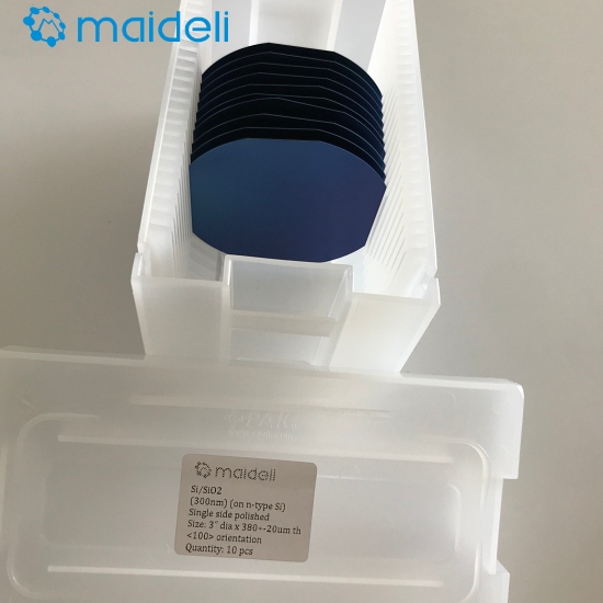
| Product | Thermal Oxide (Si+SiO2) wafers |
| Production Method | LPCVD |
| Surface Polishing | SSP/DSP |
| Diameter | 2inch / 3inch /4inch / 5inch/ 6inch |
| Type | P type / N type |
| Oxidation Layer thicnkess | 100nm ~1000nm |
| Orientation | <100> <111> |
| Electrical resistivity | 0.001-25000(Ω•cm) |
| Application | Used for synchrotron radiation sample carrier, PVD/CVD coating as substrate, magnetron sputtering growth sample, XRD, SEM, Atomic force, infrared spectroscopy, fluorescence spectroscopy and other analysis test substrates, molecular beam epitaxial growth substrates, X-ray analysis of crystalline semiconductors |
Please send us your request with below details to " sales@mdlmaterials.com"
1. Size with tolerance (Diameter / Thickness /oxidation layer thickness )
2. Type ( N or P type )
3. Orientation
4. Electrical resistivity
5. Polishing Side (SSP or DSP )
6. Quantity


