


We can provide high temperature superconducting thin film substrate, magnetic thin films and ferroelectric thin film substrate, semiconductor crystal, optical crystal, laser crystal materials, at the same time provide orientation, crystal cutting, grinding, polishing and other processing services
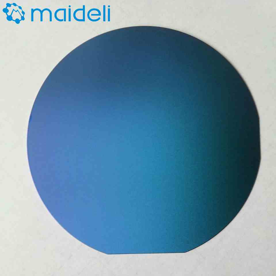
Pt/Ti/SiO2/Si single crystal wafer
Typical physical properties:
Pt layer : 150nm
Ti layer: 20nm
SiO2 layer: 300nm

Si wafer <100> P-type/B dia 4" x 0.5mm SSP
Resistivity : 2~4 ohm.cm
we can cut the wafer into : 10x10x0.5mm / 15x15x0.5mm,or other customized dimension.
The orientation of top Pt <111> film .


