


We can provide high temperature superconducting thin film substrate, magnetic thin films and ferroelectric thin film substrate, semiconductor crystal, optical crystal, laser crystal materials, at the same time provide orientation, crystal cutting, grinding, polishing and other processing services .
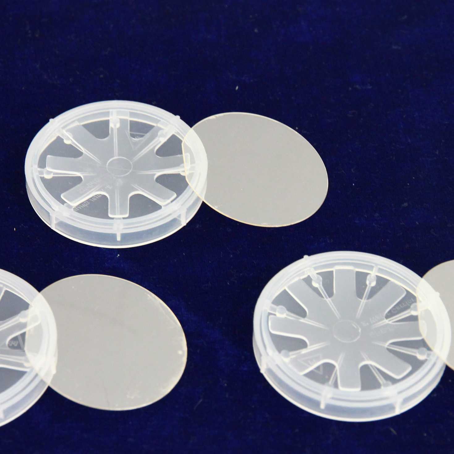
2" GaN Gallium Nitride Wafer
Specifications
| Item | GaN-T-N | GaN-T-S |
| Dimensions | Φ2 inch | |
| Thickness | 15um,20um,30um,40um | 30um,90um |
| Orientation | C-axis(0001)±1° | |
| Conduction Type | N-Type | Semi-Insulating |
| Resistivity(300K) | <0.05Ω.cm | >106Ω.cm |
| Dislocation Density | Less than 1 x108 cm-2 | |
| Substrate Structure | Thick GaN on Sapphire (0001) | |
| Useable Surface Area | >90% | |
| Polishing | Standard : SSP ( Single Side Polished ) Option: DSP(Double Sides Pollished ) | |
| Package | Package in a class 100 clean room environment ,in cassettes of 25 pcs or single wafer containers ,under a nitrogen atmosphere . | |


