


We can provide high temperature superconducting thin film substrate, magnetic thin films and ferroelectric thin film substrate, semiconductor crystal, optical crystal, laser crystal materials, at the same time provide orientation, crystal cutting, grinding, polishing and other processing services
2 Inch Free-Standing GaN Substrates
| Item | GaN-FS-N | GaN-FS-SI |
| Dimensions | Φ50mm±1mm | |
| Marco Defect Density | A Level | ≤2cm-2 |
| B Level | >2 cm-2 | |
| Thickness | 350±25um | |
| Orientation | C-axis(0001)±0.5° | |
| Orientation Flat | (1-100)±0.5°,16.0±1.0mm | |
| Secondary Orientation Flat | (11-20)±3°,8.0±1.0mm | |
| TTV(Total Thickness Variation) | ≤15um | |
| BOW | ≤20um | |
| Conduction Type | N-Type | Semi-Insulating |
| Resistivity(300K) | <0.5Ω.cm | >106 Ω.cm |
| Dislocation Density | Less than 5 x 106 cm-2 | |
| Useable Surface Area | >90% | |
| Polishing | Front Surface: Ra<0.2nm. Epi-ready polished Back Surface:Fine ground | |
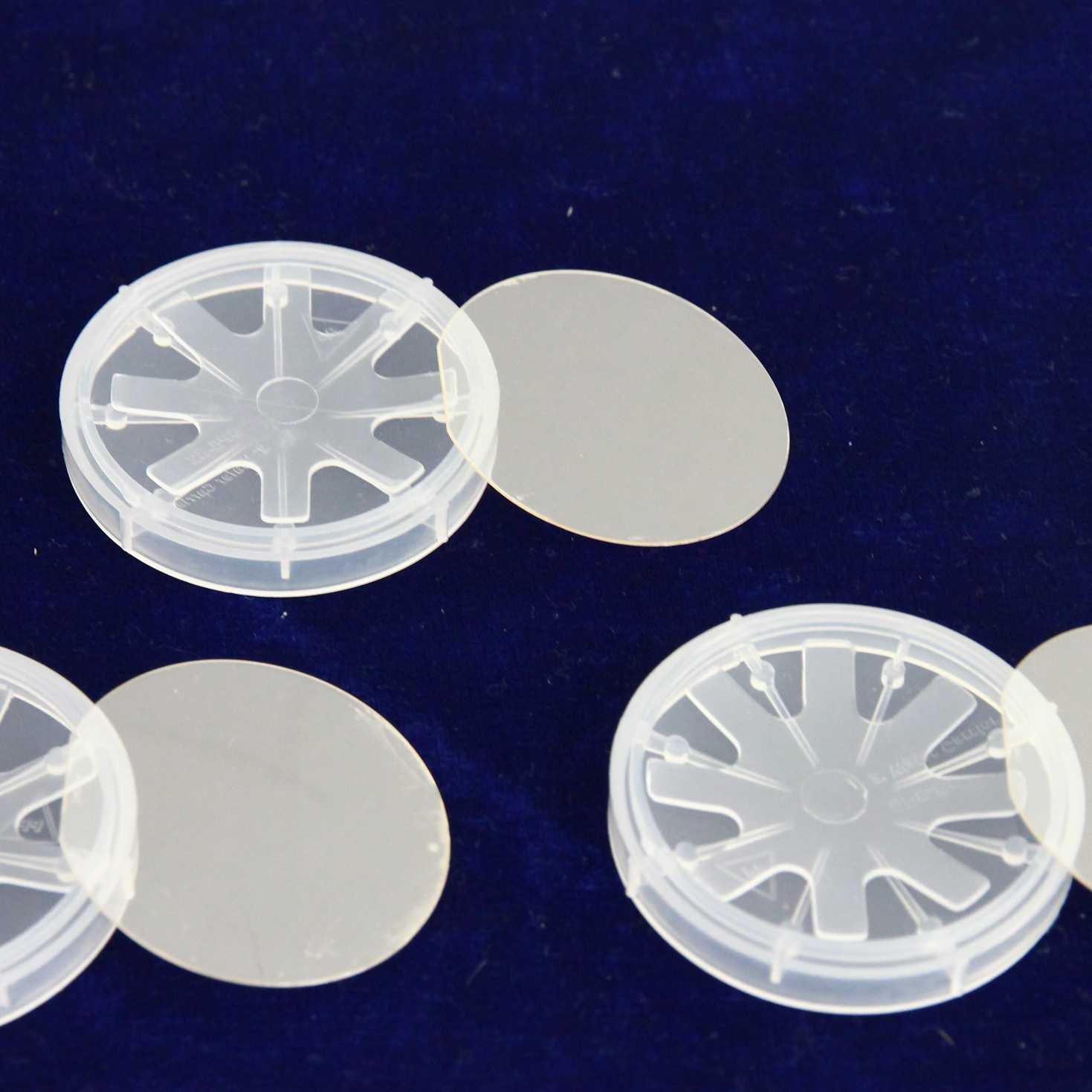
| Package | Packaged in a class 100 clean room environment ,in single wafer containers ,under nitrogen atomsphere. | |


